Raman-SPM/AFM combined systems
You can combine the power of inVia with scanning probe microscopes (SPMs and AFMs) to investigate the composition, structure and properties of materials at nanometre scales.
Choose the best system
The inVia is incredibly flexible; Renishaw can directly couple it to a wide range of AFMs and SPMs from vendors such as:
- Bruker Nano Surfaces
- Nanonics
- NT-MDT
- JPK
- Park
- Nanosurf
Choose the best SPM/AFM for your needs.

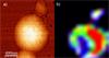
TERS: tip-enhanced Raman scattering
Selected inVia-AFM systems can perform tip enhanced Raman scattering (TERS). This exciting technique uses a sharp plasmonic tip to obtain chemical information at the nanometre scale.
TERS mapping complements StreamLine™ and StreamHR™, giving you the flexibility to study your samples at whichever resolution you like.
Maximum efficiency
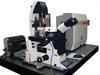
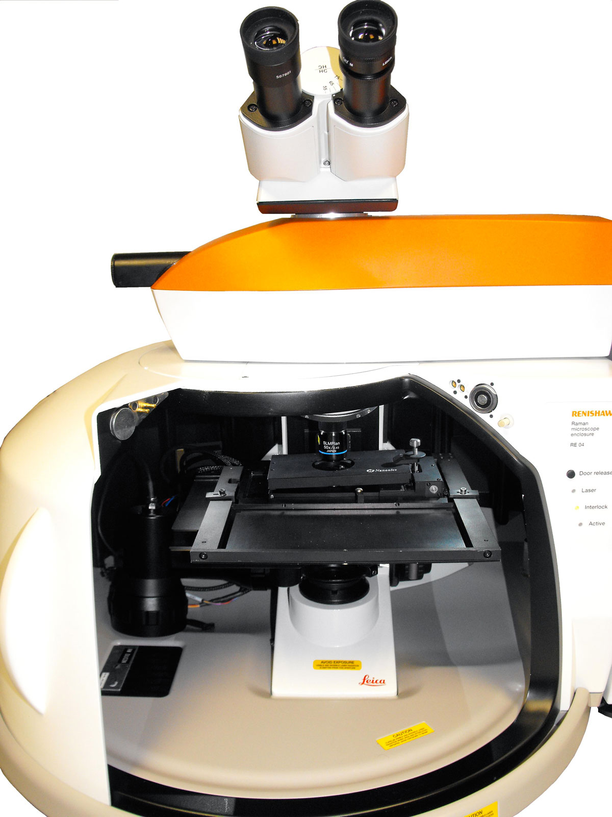
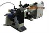
Renishaw's specially designed flexible coupling arm can be used to optically integrate inVia to SPM/AFMs. It uses mirrors to direct the light, providing a higher efficiency than fibre optic coupling. You can get your spectra faster, and with higher signal-to-noise.
Alignment is easy. All combined systems offer an inbuilt video with white light illumination so you can clearly see both the probe tip and the Raman laser spot together—critical for TERS work.
Same location, same time
You can have confidence in your data. You can simultaneously acquire Raman and AFM data from the same point on the sample without having to move it. This ensures that your data are consistent, even if your sample is changing with time.
One combined system
Analysis is co-localised; you don't have to move your sample between systems and then laboriously hunt to find the same point of interest.
Two users can operate the inVia and SPM/AFM independently and simultaneously, without any compromise in the performance of either. You have a Raman system, an SPM/AFM system and a combined Raman-SPM/AFM system.
Selecting the best system
Renishaw's SPM experts are happy to discuss your specific requirements and recommend the best way to integrate inVia to your choice of SPM/AFM system. Please contact us, and discover how this technology can extend your understanding of the nanoscale.
Download document


Image gallery


Find out more
Latest SPM/AFM user stories
The US Army Research Laboratory combines Raman and AFM
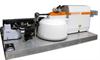
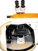
The US Army Research Laboratory (ARL) in Maryland, USA, is studying electrochemical energy storage materials with a hybrid instrument consisting of a Renishaw inVia confocal Raman microscope and a Bruker Dimension Icon atomic force microscope (AFM).
Renishaw's inVia confocal Raman microscope connects to Bruker's Dimension Icon AFM
Renishaw is an experienced supplier of integrated Raman-AFM solutions, having offered them for over 16 years. The latest addition to the range of instruments it supports is Bruker's Dimension Icon AFM. This additional pairing demonstrates the extreme flexibility of the Renishaw inVia confocal microscope, and its ability to interface to a wide range of instruments employing many analytical techniques.