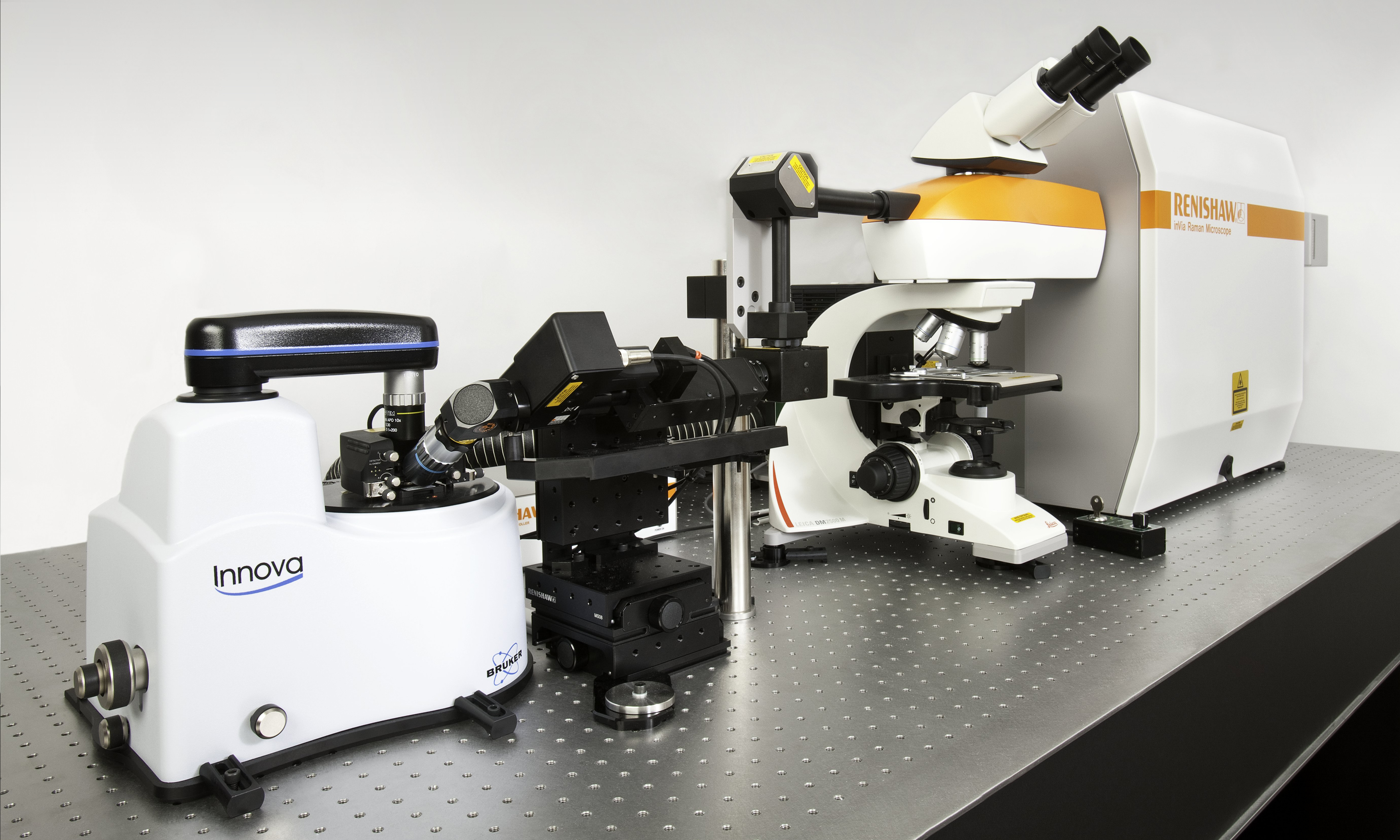
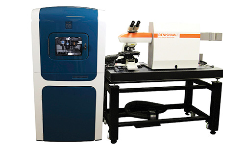
Combined Raman systems for multimodal imaging
You can couple a Renishaw inVia™ confocal Raman microscope or Virsa™ Raman analyser with other analytical instruments to gain correlative imaging capabilities. Our engineers have successfully integrated Renishaw Raman spectrometers with a wide range of analytical techniques. You can thus combine Raman spectroscopy data with information from other analysis methods including:
- Scanning electron microscopy (SEM)
- Atomic force microscopy (AFM)
- Tip-enhanced Raman spectroscopy (TERS)
- Brightfield, darkfield and polarised microscopy
- Transmitted light microscopy
- Fluorescence microscopy
- Photoluminescence (PL)
- Second-harmonic generation (SHG)
- Fluorescence lifetime imaging microscopy (FLIM)
- Time-correlated single photon counting (TCSPC)
- Infrared (IR) thermography
- Photocurrent mapping
- Nanoindentation
- Rayleigh mapping
For an efficient workflow, you can analyse your sample with two or more characterisation techniques on a single integrated instrument. With Renishaw's correlative microscopy solutions, you can be confident that you are analysing the same point with more than one technique. Explore some of our combined Raman systems below.
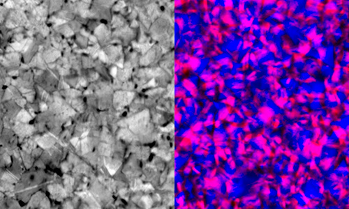
Second-harmonic generation (SHG)

Polarised SHG image of MoS2. The image shows the variation in SHG intensity which is a function of crystal orientation. We used StreamHR™ Rapide imaging technology to collect SHG data in just 9 minutes using step sizes of 200 nm.
SHG is a fast technique that provides complementary information to Raman spectroscopy. It is important for investigating 2D materials for nano-optics and optoelectronics applications, as well as biological imaging. Another common use of SHG is to identify regions of interest for detailed Raman analysis. For example, SHG can identify regions rich in fibrillar collagen in biological tissues.
Contact us to find out more about our integrated SHG solution for inVia Raman microscopes.
Contact us
External triggering for Raman analysis
Synchronise and automate your Raman measurements using an external trigger. Find out how a Renishaw Raman system can interface with third-party hardware or software.
See more

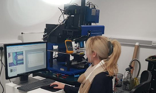
SPM/AFM Raman
You can combine the inVia™ Raman microscope with a wide range of scanning probe microscopes (SPMs) and atomic force microscopes (AFMs) to reveal complementary information such as topography and mechanical properties. Add tip-enhanced Raman spectroscopy (TERS) for nanometre-scale chemical resolution.
See more
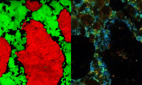
Fluorescence lifetime imaging microscopy (FLIM)
FLIM can be integrated with an inVia Raman microscope to collect a spatial image showing the fluorescence lifetime of a fluorophore. FLIM is used in cell biology for environmental sensing, monitoring molecular interactions, and fluorophore identification.
See more
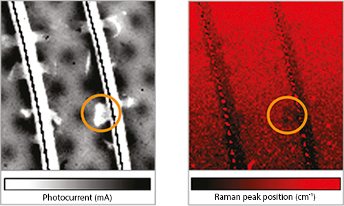
Photocurrent imaging
Equip your inVia confocal Raman microscope to map photocurrents generated from the incident laser light. Photocurrent mapping of photovoltaic devices reveals the electronic, optical, and charge transport properties of the material.
See more
Photoluminescence
Use photoluminescence (PL) to study the electronic properties of materials. You can configure your inVia microscope to study crystal defects, atomic vacancies and substitutions. PL is useful for analysing materials like photovoltaics, semiconductors and gemstones.
See more
Nanoindentation
Combine the power of the inVia Raman microscope with nanoindentation measurements and directly correlate mechanical and tribological properties with chemical information such as crystallinity, polymorphism, phase and stress.
See more
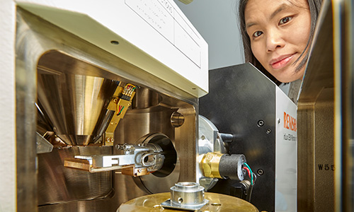
inLux™ SEM Raman interface
The inLux SEM Raman interface brings high-quality Raman functionality to your SEM chamber. Now you can collect Raman images in 2D and 3D whilst simultaneously collecting high-resolution SEM images.
See more
Medium wavelength infrared (MWIR) Raman thermography
The Virsa analyser can be fibre-coupled with a MWIR temperature measurement microscope. Use Raman thermography on semiconductor devices to determine the local temperature with submicron lateral spatial resolution.
See more
Other custom solutions
If our standard products don't match your exact needs, our Special Products Team are experienced at developing custom solutions to meet user requirements. Explore examples of Raman integration at synchrotron beamlines and routine QA/QC analysis environments.
See more
Spectroscopy eBook: The Latest Advances in Correlative Raman Imaging
Raman spectroscopy is a rapidly expanding field, with modern Raman spectrometers offering labs higher ease-of-use and sensitivity. Learn how you can combine Raman spectroscopy with scanning electron microscopy (SEM) or fluorescence-lifetime imaging microscopy (FLIM), thus enhancing the technique for various applications.
- Developments in Raman instrumentation and the innovations of Raman technology;
- In-situ Raman spectroscopy within a SEM chamber, and how the inLux SEM Raman interface provides complementary information during SEM imaging;
- Correlative FLIM and Raman microscopy, with examples of imaging on plant tissue sections and HeLa cells.
Spectroscopy eBook download
Download document

On-demand webinar: Combining Raman spectroscopy with other techniques, for data rich science
Raman spectroscopy is often one tool amongst the many required to solve complex research challenges. Renishaw has developed the inVia microscope to be used in conjunction with other techniques, to collect correlated data and to build a better picture of the science underpinning your samples. In this webinar, we will present Raman data collected in conjunction with other techniques such as photocurrent measurements, PL, SEM, AFM, topography measurements, and Rayleigh scattering.
Want to find out more?
Your local representative will be happy to help with your enquiry.
You can contact them by completing a form or sending an email.
Contact Us
Get our latest updates
Stay up-to-date with our latest news, webinars, application notes and product launches delivered directly to your inbox.
Subscribe