Tato stránka není v současné době k dispozici ve vašem jazyce. Automatizovaný překlad můžete zobrazit pomocí nástroje Google Translate. Neodpovídáme za poskytování této služby a výsledky překladu jsme nekontrolovali.
Potřebujete-li další pomoc, kontaktujte nás.
What links metrology with solar energy?
Solar growth
Power generation from solar cells - also known as photovoltaic (PV) cells - has grown significantly in popularity over the last decade and shows no sign of fading. The application of solar technology is vital for smart grids, distributed power generation and the full participation of consumers in the energy market. In the near-term, large-scale solar power generation is becoming increasingly popular and now competes on a price-per-kilowatt basis with traditional energy sources such as nuclear and gas.
Growth in the solar power market has shown a significant upturn in recent years with a 50 % growth in installed capacity between 2015 and 2016. China is the largest market and was responsible for nearly half of this new capacity. The Asia-Pacific (APAC) area has now become the largest solar-powered region in the world with 147.2 GW of total installed capacity (2016), exceeding that of Europe and the US.
Growth of the global solar market is likely to slow in the next few years as regulatory frameworks, new market designs and infrastructure investment catch up. However, high growth rates are likely to return by the early 2020s as solar becomes the cheapest available power generation technology at large-scales (Figure 1). In the longer term, distributed ‘rooftop' solar power generation on both residential and commercial buildings should gain substantial market share.
According to SolarPower Europe, who represent members active in the solar industry, almost 1 TW (Terawatt) of global installed solar power is possible by 2021. Furthermore, the EU will need to reach a target of a least 35 % renewable energy sources (RES) by 2030 to meet its commitment to cut domestic greenhouse gas emissions to 20% of 1990 levels by 2050. There is likely to be ever increasing demand for photovoltaics over the coming years with solar cell manufacturers and others in the solar supply chain facing significant growth opportunities.

Fig 1: large scale solar power installation
PV manufacturing
Due to the high-volume nature of PV manufacturing, fully automated end-to-end production is commonplace. The standard monocrystalline PV cell is a p-doped silicon (Si) substrate (absorber) with a thin n-doped surface layer and an anti-reflection coating. The barrier between the n and p-type semiconductors is called a p-n junction and allows the accumulation of electrons and holes (positive charges) on opposite sides without recombination.
When light is incident on a PV cell, it liberates charge which then flows to the cell terminals, thereby producing an open-circuit voltage. Multiple cells are combined in a solar module and subsequently linked with other modules to generate significant power (Figure 2).
The basic solar panel manufacturing process is summarised as follows:
- Input of Si wafer
- Surface texturing (reduces reflections)
- p-n junction formation (wet chemistry)
- Oxide etch (removal of unwanted surface layer)
- Anti-reflective coating
- Metal contact printing (screen printing)
- Metal contact heat treatment (cofiring)
- Edge isolation (laser ablation)
- Testing and sorting
Motion control is required at every step and all handling steps in-between. One of the most challenging processes is the precise deposition of the metal contact layers. Silver and aluminium paste is screen printed on the front and back surfaces of each wafer. The sunward side of the PV cell has a printed series of fine contact fingers approximately 100 microns wide, with a pitch of 2 mm, overlaid with two or three perpendicular bus bars. The rear side has a corresponding set of bus bars over a metalized area. The main function of the front and rear bus bars is to collect the current and to enable mechanical contact with conducting electrodes.
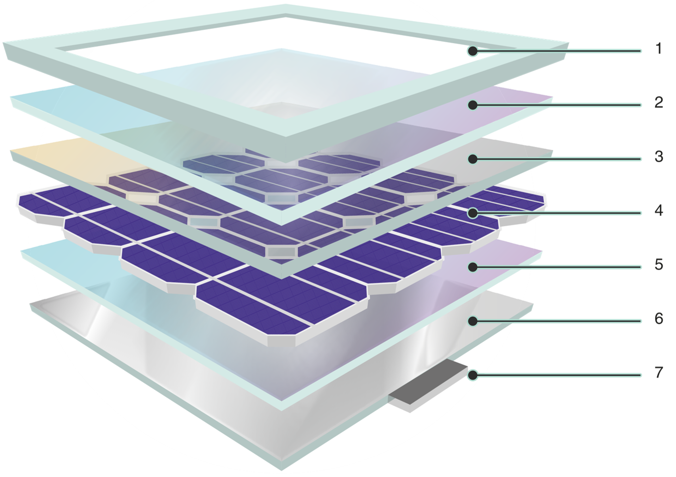 Fig 2: component parts of a solar module
1 = Frame
2 = Glass
3 = Encapsulant
4 = Solar cells
5 = Encapsulant
6 = Backsheet
7 = Junction box
A screen printing system for PV applications may utilise the following steps:
- Wafer inspection - The system delivers the wafer to an inspection zone and images at least two fiducials (alignment marks) on the upper surface of the wafer.
- Image processing - Precise position data for each fiducial is then determined by image processing software and periodically updated in memory to improve accuracy over many printed layers.
- Wafer alignment - The wafer stage is finely adjusted in X, Y and θ (see Figure 3) to correct for offsets and then transferred beneath a mesh printing screen (stencil). These adjustments overlap the fiducials on the wafer with the stored reference fiducials. Both linear and angular encoders provide the requisite position feedback to drive each axis to accurately align the wafer with the screen.
- Printing - After alignment, the wafer is clamped in place before direct application of silver and aluminium paste by conventional screen printing.
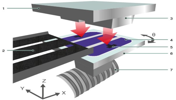
Fig 3: wafer screen printing system
1 = Image processing unit
2 = Fixed print screen
3 = Camera
4 = Wafer
5 = Fiducial
6 = Wafer stage
7 = Leadscrew
Motion control requirements
Current monocrystalline PV cell efficiencies approach 20 %: the maximum theoretical limit is about 29 % for a silicon single-junction cell. Improvements to conversion efficiency drive down costs per KWh and reduce the physical footprint of solar power installations, so manufacturers are constantly improving their production processes to achieve efficiency gains.
A typical silicon solar cell production process requires multiple screen printing runs, and there are at least two separate printing steps for the front and back sides of the cell. For improved efficiency, contact lines on the front side must be printed as finely as possible without reducing conductivity, which requires the printing of layers that are overlaid with high accuracy and repeatability.
By making the lines thinner and taller, more of the cell can participate in solar energy conversion (Figure 4). For instance, moving from contact fingers with 120 µm line width to 70 µm line width, with twice the thickness, gives a potential conversion efficiency gain of 0.5 %. Another technique for improving performance is the use of selective emitters - the n-doped front side of the solar cell. By strongly doping the area directly below the metal contacts and only weakly doping the other areas, cell efficiency at shorter wavelengths can be improved (Figure 5).
There are several techniques available for manufacturing selective emitters and most involve the highly-accurate alignment and deposition of layers. Screen alignment accuracy is the most critical metric for multi-layer printed contacts because subsequent print layers must be precisely placed over the first. State-of-the-art alignment systems with high-resolution cameras are now capable of ±10 µm alignment accuracy. High-precision position encoders, such as Renishaw's RESOLUTE absolute encoder system, are key to improving print screen overlay accuracy and control. RESOLUTE encoders are capable of high translational speeds to 100 m/s, high resolutions to 1 nm, and low cyclic error of ±40 nm.
-
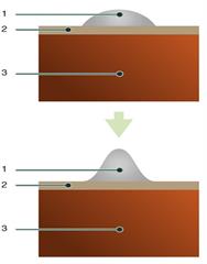 Fig 4: reduction of the line width of metal contact fingers increases solar cell efficiency
(1 - Metal contact, 2 - Doped margin, 3 - Substrate)
-
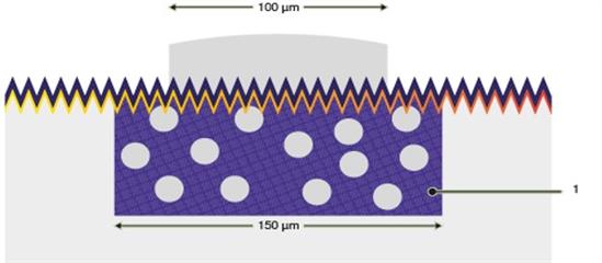 Fig 5: a large n-doped region under each metal contact
(1 - Selective emitter n-doped region)
Summary
Solar energy is likely to become a major source of electrical power over the coming decades with applications in both centralised and distributed generation e.g. rooftop solar (Figure 6). There are many commercial opportunities for successful supply chain participants. Motion control is involved at every stage of the manufacturing process of PV cells and is particularly essential for high-precision screen printing. Renishaw's motion control expertise and extensive encoder product ranges provide OEMs and end users with the latest metrology solutions for their motion control needs.
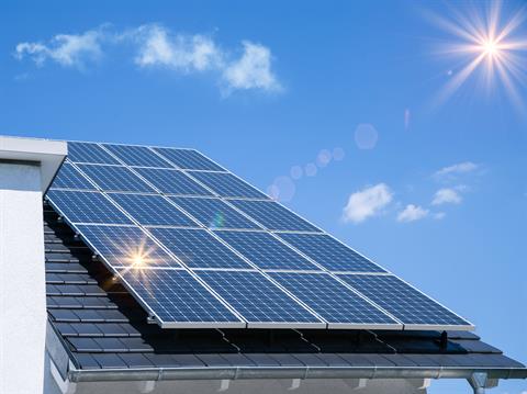
Fig 6: rooftop solar panels

