White light and Raman images of a silicon wafer indented with a diamond tip at high temperature and pressure (jpg)
File size: 273 kB
Language: Language Independent
Dimensions: 1500 x 567 px
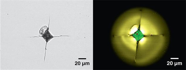
The microscope white light image shows the location and appearance of the indentation. The Raman map reveals changes in structure, composition, and stress. At the indentation site, crystalline silicon IV has been transformed to amorphous silicon (green), and small spots of silicon carbide (red) have formed. Compressive (light yellow) and tensile (dark yellow) stresses are also revealed, as is the absence of stress along the cracks (black). Data courtesy of G K Banini, University of Cambridge, UK.
Latest videos - Raman spectroscopy


Didn't find what you were looking for?
Tell us what you couldn’t find and we will do our best to help.